![New Industry Creation Hatchery Center[NICHe]](../img/common/niche_en.svg)
Development of Crystals and Application Devices Contributing to Sustainable Society
 ProfessorAkira Yoshikawa
Research Overview
This project is characterized by the fusion of different fields of physics and chemistry, science and engineering. Through an industry-academia collaboration system that vertically integrates elemental technologies from upstream (material design) to downstream (device development), we are developing new functional crystals for implementation into society.
Currently, we are focusing on scintillators, next-generation power semiconductors, difficult-to-process alloys (wire and plate), and piezoelectric materials. We are also developing fabrication methods for crystals that have unique properties, but which are difficult to synthesize using conventional procedures or are difficult to produce on an industrial scale.
Research Features
When developing single crystals, we screen materials by evaluating their response to external stimuli such as light, radiation, pressure, and heat, as well as their piezoelectric properties using high-precision ultrasonic measurement technology, and also by promptly feeding back the results. In doing so, we target the development and improvement of the characteristics required by users by designing upstream materials based on the requirements of downstream devices. For crystals with special properties, we are also proactively involved in social implementation activities, such as device realization and mounting actual devices into applications, by establishing an industry-academia collaborations. Several Tohoku University venture companies have been spun off based on our laboratory results.
Expected Outcomes and Developments
This project conducts research and development with practical applications in mind, and is currently carrying out research mainly on the following research topics while promoting social implementation in cooperation with companies in Japan and overseas.
- Development of a new noble metal crucible-free crystal growth method using AI calculations to establish a high-quality substrate fabrication technology for gallium oxide single crystals for next-generation power semiconductors (MEXT program)
- Development of functional single crystals using an innovative noble metal crucible-free single crystal fabrication method. (NEDO Program)
- Development of an ultra-high resolution and high sensitivity optical waveguide scintillator detector that will revolutionize X-ray imaging (FY2024 Go-Tech Program)
- Development of innovative neutron/γ scintillation detection system for simple nondestructive measurement (CLADS Program)
- Development of novel scintillator for forceps-type mini PET enabling pre-resection lymph node diagnosis during cancer surgical treatment (Fukushima Regional Reconstruction Program)
- Innovative manufacturing alloy wire method for three-dimensional laminated fabrication (Fukushima Regional Reconstruction Program)
- Development of compact and lightweight position-sensitive radiation detector for imaging (NEDO Program)
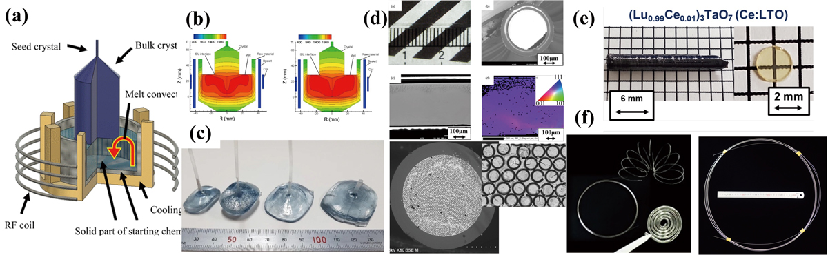
(a) OCCC method (crystal growth that is free from precious metal crucibles) (b) simulation of temperature distribution of melt in OCCC method (c) gallium oxide crystals grown by OCCC method (d) optical-guiding crystal scintillator (OCS) (e) Ce:LTO single crystal with ultra-high melting point grown in a W crucible (f) Ir wire grown by alloy micro-PD (pulling down) method