Development of Advanced Optical / Electronic Devices Using Nitride Semiconductors
2026/4/1 - 2029/3/31
 Senior Research FellowTakashi Matsuoka
Research Overview
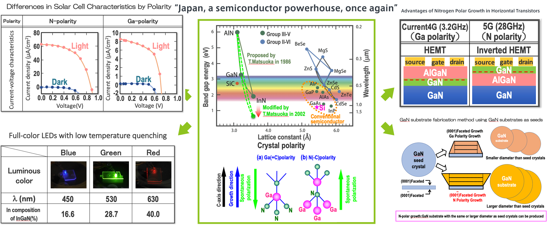
We are conducting materials research with the creation of devices in mind. Nitride semiconductors proposed by Project Leader, Professor Emeritus Takashi Matsuoka of Tohoku University in 1986 are already used in blue LEDs and transistors for base stations of cellar phones. Currently, we are developing epitaxial growth technology of nitride semiconductors on several substrates such as ScAlMgO4, red LEDs with low temperature quenching, high-efficiency/high-power transistors that can operate in the millimeter-wave band or higher for post-5G applications. Recently, we have proposed “complimentary transistors” fabricated by one-time epitaxial growth without any impurity doping. The results obtained will be transferred to industry.
Research Features
- R&D style: materials and their epitaxial growth to device fabrication
- Research group composition: from material scientists to device specialist
- Equipment: materials and thin film evaluation, metalorganic vapor deposition, device fabrication, and device evaluation
- Technology:
- Semiconductor lasers currently used in optical fiber communications systems: Distributed Feedback (DFB) lasers
World's first room temperature continuous oscillation, transfer of fabrication technology to manufacturer, introduction of system
This laser has increased the communication capacity of 100,000 compared with the earlier Fabri·Perot (FP) laser and realized advance information society. - Nitride semiconductor InGaAlN
Blue light-emitting diode:
InGaAlN proposal, world's first light-emitting material InGaN growth
Unexplored terminal material InN:
Single crystal thin film growth, Band gap energy corrected from 2eV to 0.7eV
Proposal of crystalline polarity and polarity-controlled epitaxial growth
Epitaxial growth technology
Metalorganic vapor phase epitaxy (MOVPE) system: design and operation - World's fastest transistor:
High reliability, high breakdown voltage, and integration with optical elements; twice broke the cutoff frequency record for InP-based high electron mobility transistors.
Expected Outcomes and Developments
- “Horizontal transistors” for 5G/6G base stations
Advanced communication technologies such as cell phone communication or two-way communication in automobiles (connected car). - High-output, high-voltage “vertical transistors” for automobiles
The current Si chip in a cooling mechanism in electric vehicle motor drives which can be replaced by electronics not requiring a cooling mechanism, and enables higher efficiency and smaller size circuits - GaN single-crystal substrates
Low-cost large GaN substrates for “vertical transistors” - Red LEDs made of nitride semiconductors
Replacing current InGaAlP-based red LEDs, which require air cooling, with low-cost, low-power full-color displays that require no cooling mechanism
Realization of low-cost, low-power-consumption full-color displays that require no cooling mechanism - High-power laser diodes
Realization of underwater communication by welding metals such as copper and blue - Compound semiconductor high-frequency devices
Realization of terahertz transistors exceeding 300 GHz, applied to measurement devices for communication equipment for 5G/6G and terahertz light sources that enable radiation exposure-free, non-destructive, security inspection - Complimentary transistors
First application of nitride semiconductor transistors to logic circuits with high speed and low power consumption