![New Industry Creation Hatchery Center[NICHe]](../img/common/niche_en.svg)
Center for Holistically Integrated and Packaged Systems (Tohoku CHIPS)
 ProfessorTakafumi Fukushima
Research Overview
Based on three-dimensional stacked integrated circuits (3D-IC) and chiplet technology pioneered at Tohoku University, we are conducting research and development on the integration of next-generation semiconductor systems by making full use of advanced semiconductor packaging engineering (Advanced Microelectronic Packaging Engineering) accumulated over the past 30 years. We are developing the integration of next-generation semiconductor systems. In addition to “elemental integration,” which enhances the performance of individual components, we focus on “holistic integration,” which encompasses chip-to-chip wiring, mounting methods, and heat dissipation design.
Research Features
GINTI (Global INTegration Initiative), which is a 3D superchip LSI prototyping and manufacturing base jointly operated with Tohoku Microtech, is a university-based startup company that can flexibly fabricate 3D-ICs using 200-300 mm-diameter Si wafers, the standard for semiconductor R&D. Our project differentiates itself from others with a technology that enables “rapid prototyping of 3D-ICs” using die-level and multi-chip-level 3D packaging, which is unprecedented in the world. This project also aims to transform GINTI, which is the sole prototyping center, into an “open innovation center” and to play a role in the revival of Japan's semiconductor industry by strengthening cooperation with industry, government, and academia in Japan and overseas.
Expected Outcomes and Developments
Through the formation of Through-Si Via (TSV) on 2D-IC chips to create 3D-ICs and heterogeneous integration with optoelectronics, we are pioneering the “mid-process” area that integrates front-end and back-end semiconductor processes and is the most important area in the industry. By establishing a technology base for design, materials, processes, and reliability analysis, we will build a technological foundation that will promote higher performance and multifunctionality of the entire semiconductor system, including not only the inside of integrated circuits, but also the package boards outside of integrated circuits and the interposers (relay boards) that connect them. In addition to 3D-integration of logic chips, functional verification of innovative 3D-ICs, such as logic chips with integrated logic and digital chips and 3D-AI chips, can be demonstrated in a short period of time, and the introduction of new architectures can be accelerated. Furthermore, technologies that contribute to high-mix, high-volume production, such as massively parallel assembly of chiplets, will be brought to a practical level and the integration of heterogeneous devices will be advanced. Through these efforts, we expect to further broaden the base of Japan's semiconductor industry, contribute to human resource development, and help to create a semiconductor market that is not solely occupied by mega-fabs.
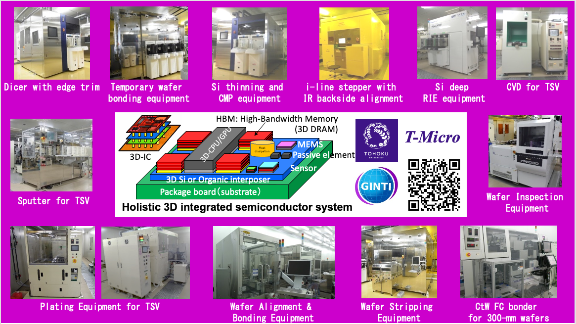
Conceptual diagram of holistic 3D-integrated semiconductor system and GINTI’s equipment line to develop an integrated 3D-IC manufacturing line using 300-mm wafers
Current Status and Future Prospects of 3D-integrated semiconductors(3D-ICs) for Future Industries - From activities of GINTI, a 3D-IC research and development center at Tohoku University-
https://youtu.be/3zPtmCtSOJg
Please feel free to view the YouTube video and subscribe.