![New Industry Creation Hatchery Center[NICHe]](../img/common/niche_en.svg)
Development of Evaluation Technology Contributing to the Creation of Materials and Devices for Next-Generation Innovative Power Electronics Using Scanning Nonlinear Dielectric Microscopy
 Specially appointed ProfessorYasuo Cho
Research Overview
The core technology of this project is the Scanning Nonlinear Dielectric Microscope (SNDM), which was developed in Japan by the Principal Investigator of this project.
In this project, we will solidify Japan's industrial competitiveness in the power electronics field by creating and applying unique nanoscale measurement technologies, such as nanoscale and atomic-scale evaluation of interface defects, which are the cause of reduced reliability in devices, including reduced channel mobility and threshold instability.
Research Features
The evaluation of next-generation and future-generation power devices using wide-gap semiconductors has been conducted mainly by macroscopic methods without spatial resolution, such as measuring capacitance-voltage (C-V) characteristics of wafers and electrical characteristics of devices. In contrast, this research method enables nanoscale and atomic-scale characterization of crystal defect distribution for high-quality crystal growth, activated dopant distribution for impurity concentration control technology, and density distribution of interface defects and their atomic structures that cause reliability degradation such as low channel mobility and threshold instability. SNDM can also be used to evaluate dielectric properties. SNDM has the world's highest sensitivity and resolution in dielectric measurement, enabling detailed analyses of nano-scale polarization distribution and other unique material features.
Expected Outcomes and Developments
The establishment of semiconductor and dielectric analytical microscopy with ultra-high sensitivity, high functionality, high spatial resolution, and high temporal resolution, will greatly advance the research and development of next-generation power semiconductor materials and devices and dielectric passive devices. The research results obtained from this project will be applied to power semiconductors as well as to dielectric passive devices.
Furthermore, the research results obtained will contribute not only to the development of power semiconductors, but also to the technological development of integrated circuits, communication semiconductors, and dielectrics, and will advance Japan's semiconductor industry to take the lead again toward Beyond 5G (6G).
The results of this project will be mainly deployed in the semiconductor and dielectric industries, and are expected to contribute not only to industrial applications but also to Japan’s academic community, including manufacturers of evaluation and analysis instruments such as probe microscopes.
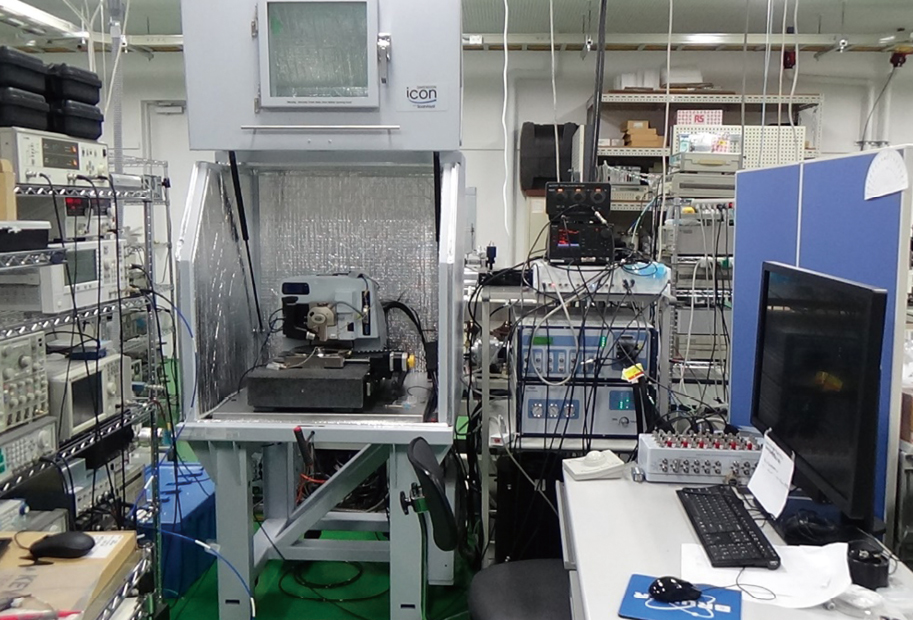
Developed scanning nonlinear dielectric microscope system
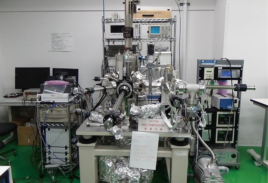
Developed atomic resolution scanning nonlinear dielectric microscope system